- 您现在的位置:买卖IC网 > Sheet目录1998 > ICS873995AYLF (IDT, Integrated Device Technology Inc)IC ZD/MULT/DIVIDER 48-LQFP
IDT / ICS LVPECL ZERO DELAY/MULTIPLIER/DIVIDER
10
ICS873995AY REV. A SEPTEMBER 11, 2008
ICS873995
DIFFERENTIAL-TO-3.3V LVPECL ZERO DELAY/MULTIPLIER/DIVIDER
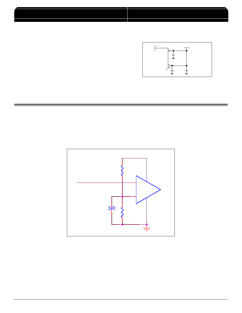
Figure 2 shows how the differential input can be wired to accept
single ended levels. The reference voltage V_REF = V
CC
/2 is
generated by the bias resistors R1, R2 and C1. This bias circuit
should be located as close as possible to the input pin. The ratio
FIGURE 2. SINGLE ENDED SIGNAL DRIVING DIFFERENTIAL INPUT
WIRING THE DIFFERENTIAL INPUT TO ACCEPT SINGLE ENDED LEVELS
of R1 and R2 might need to be adjusted to position the V_REF in
the center of the input voltage swing. For example, if the input
clock swing is only 2.5V and V
CC
= 3.3V, V_REF should be 1.25V
and R2/R1 = 0.609.
V_REF
R1
1K
C1
0.1u
R2
1K
Single Ended Clock Input
CLKx
nCLKx
VCC
As in any high speed analog circuitry, the power supply pins
are vulnerable to random noise. The ICS873995 provides sepa-
rate power supplies to isolate any high switching
noise from the outputs to the internal PLL. V
CC, VCCA and
V
CCOx
should be individually connected to the power supply plane
through vias, and bypass capacitors should be used for each
pin. To achieve optimum jitter performance, power supply iso-
lation is required.
Figure 1 illustrates how a 10
Ω resistor along
with a 10
μF and a .01μF bypass capacitor should be connected
to each V
CCA pin.
FIGURE 1. POWER SUPPLY FILTERING
10
Ω
V
CCA
10
μF
.01
μF
3.3V
.01
μF
V
CC
POWER SUPPLY FILTERING TECHNIQUES
发布紧急采购,3分钟左右您将得到回复。
相关PDF资料
ICS874001AGI-02LF
IC PCI EXPRSS/JITT ATTEN 20TSSOP
ICS874001AGI-05LFT
IC PCI EXPRSS/JITT ATTEN 20TSSOP
ICS874002AGLFT
IC PCI EXPRSS/JITT ATTEN 20TSSOP
ICS874005AG-04LFT
IC PCI EXPRSS/JITT ATTEN 24TSSOP
ICS874005AGLFT
IC PCI EXPRSS/JITT ATTEN 24TSSOP
ICS8741004AGLFT
IC PCI EXPRSS/JITT ATTEN 24TSSOP
ICS87604AGILF
IC CLK MULT/ZD BUFFER 28-TSSOP
ICS8761CYLFT
IC CLK GEN PCI/PCI-X 64-LQFP
相关代理商/技术参数
ICS873995AYLFT
功能描述:IC ZD/MULT/DIVIDER 48-LQFP RoHS:是 类别:集成电路 (IC) >> 时钟/计时 - 时钟发生器,PLL,频率合成器 系列:HiPerClockS™ 标准包装:1,000 系列:- 类型:时钟/频率合成器,扇出分配 PLL:- 输入:- 输出:- 电路数:- 比率 - 输入:输出:- 差分 - 输入:输出:- 频率 - 最大:- 除法器/乘法器:- 电源电压:- 工作温度:- 安装类型:表面贴装 封装/外壳:56-VFQFN 裸露焊盘 供应商设备封装:56-VFQFP-EP(8x8) 包装:带卷 (TR) 其它名称:844S012AKI-01LFT
ICS873996AYLF
功能描述:IC ZD/MULT/DIVIDER 48-LQFP RoHS:是 类别:集成电路 (IC) >> 时钟/计时 - 时钟发生器,PLL,频率合成器 系列:HiPerClockS™ 标准包装:2,000 系列:- 类型:PLL 频率合成器 PLL:是 输入:晶体 输出:时钟 电路数:1 比率 - 输入:输出:1:1 差分 - 输入:输出:无/无 频率 - 最大:1GHz 除法器/乘法器:是/无 电源电压:4.5 V ~ 5.5 V 工作温度:-20°C ~ 85°C 安装类型:表面贴装 封装/外壳:16-LSSOP(0.175",4.40mm 宽) 供应商设备封装:16-SSOP 包装:带卷 (TR) 其它名称:NJW1504V-TE1-NDNJW1504V-TE1TR
ICS873996AYLFT
功能描述:IC ZD/MULT/DIVIDER 48-LQFP RoHS:是 类别:集成电路 (IC) >> 时钟/计时 - 时钟发生器,PLL,频率合成器 系列:HiPerClockS™ 标准包装:1,000 系列:- 类型:时钟/频率合成器,扇出分配 PLL:- 输入:- 输出:- 电路数:- 比率 - 输入:输出:- 差分 - 输入:输出:- 频率 - 最大:- 除法器/乘法器:- 电源电压:- 工作温度:- 安装类型:表面贴装 封装/外壳:56-VFQFN 裸露焊盘 供应商设备封装:56-VFQFP-EP(8x8) 包装:带卷 (TR) 其它名称:844S012AKI-01LFT
ICS874001AGI-02LF
功能描述:IC PCI EXPRSS/JITT ATTEN 20TSSOP RoHS:是 类别:集成电路 (IC) >> 时钟/计时 - 专用 系列:FemtoClock™, PCI Express™ (PCIe) 标准包装:1,500 系列:- 类型:时钟缓冲器/驱动器 PLL:是 主要目的:- 输入:- 输出:- 电路数:- 比率 - 输入:输出:- 差分 - 输入:输出:- 频率 - 最大:- 电源电压:3.3V 工作温度:0°C ~ 70°C 安装类型:表面贴装 封装/外壳:28-SSOP(0.209",5.30mm 宽) 供应商设备封装:28-SSOP 包装:带卷 (TR) 其它名称:93786AFT
ICS874001AGI-02LFT
功能描述:IC PCI EXPRSS/JITT ATTEN 20TSSOP RoHS:是 类别:集成电路 (IC) >> 时钟/计时 - 专用 系列:FemtoClock™, PCI Express™ (PCIe) 标准包装:1,500 系列:- 类型:时钟缓冲器/驱动器 PLL:是 主要目的:- 输入:- 输出:- 电路数:- 比率 - 输入:输出:- 差分 - 输入:输出:- 频率 - 最大:- 电源电压:3.3V 工作温度:0°C ~ 70°C 安装类型:表面贴装 封装/外壳:28-SSOP(0.209",5.30mm 宽) 供应商设备封装:28-SSOP 包装:带卷 (TR) 其它名称:93786AFT
ICS874001AGI-05LF
功能描述:IC PCI EXPRSS/JITT ATTEN 20TSSOP RoHS:是 类别:集成电路 (IC) >> 时钟/计时 - 专用 系列:FemtoClock™, PCI Express™ (PCIe) 标准包装:1 系列:- 类型:时钟/频率发生器,多路复用器 PLL:是 主要目的:存储器,RDRAM 输入:晶体 输出:LVCMOS 电路数:1 比率 - 输入:输出:1:2 差分 - 输入:输出:无/是 频率 - 最大:400MHz 电源电压:3 V ~ 3.6 V 工作温度:0°C ~ 85°C 安装类型:表面贴装 封装/外壳:16-TSSOP(0.173",4.40mm 宽) 供应商设备封装:16-TSSOP 包装:Digi-Reel® 其它名称:296-6719-6
ICS874001AGI-05LFT
功能描述:IC PCI EXPRSS/JITT ATTEN 20TSSOP RoHS:是 类别:集成电路 (IC) >> 时钟/计时 - 专用 系列:FemtoClock™, PCI Express™ (PCIe) 标准包装:1,500 系列:- 类型:时钟缓冲器/驱动器 PLL:是 主要目的:- 输入:- 输出:- 电路数:- 比率 - 输入:输出:- 差分 - 输入:输出:- 频率 - 最大:- 电源电压:3.3V 工作温度:0°C ~ 70°C 安装类型:表面贴装 封装/外壳:28-SSOP(0.209",5.30mm 宽) 供应商设备封装:28-SSOP 包装:带卷 (TR) 其它名称:93786AFT
ICS874002AGLF
功能描述:IC JITTER ATTENUATOR 20-TSSOP RoHS:是 类别:集成电路 (IC) >> 时钟/计时 - 专用 系列:HiPerClockS™, PCI Express® (PCIe) 标准包装:1 系列:- 类型:时钟/频率发生器,多路复用器 PLL:是 主要目的:存储器,RDRAM 输入:晶体 输出:LVCMOS 电路数:1 比率 - 输入:输出:1:2 差分 - 输入:输出:无/是 频率 - 最大:400MHz 电源电压:3 V ~ 3.6 V 工作温度:0°C ~ 85°C 安装类型:表面贴装 封装/外壳:16-TSSOP(0.173",4.40mm 宽) 供应商设备封装:16-TSSOP 包装:Digi-Reel® 其它名称:296-6719-6